
- English
- Español
- Português
- русский
- Français
- 日本語
- Deutsch
- tiếng Việt
- Italiano
- Nederlands
- ภาษาไทย
- Polski
- 한국어
- Svenska
- magyar
- Malay
- বাংলা ভাষার
- Dansk
- Suomi
- हिन्दी
- Pilipino
- Türkçe
- Gaeilge
- العربية
- Indonesia
- Norsk
- تمل
- český
- ελληνικά
- український
- Javanese
- فارسی
- தமிழ்
- తెలుగు
- नेपाली
- Burmese
- български
- ລາວ
- Latine
- Қазақша
- Euskal
- Azərbaycan
- Slovenský jazyk
- Македонски
- Lietuvos
- Eesti Keel
- Română
- Slovenski
- मराठी
- Srpski језик

High-density packaging technology in PCBA processing
2024-08-22
High-density packaging technology in PCBA processing is an important part of modern electronic manufacturing. It realizes smaller and lighter electronic product design by increasing the density of components on the circuit board. This article will explore the high-density packaging technology in PCBA processing in depth, including its definition, application, advantages, and related challenges and solutions.
1. Definition of high-density packaging technology
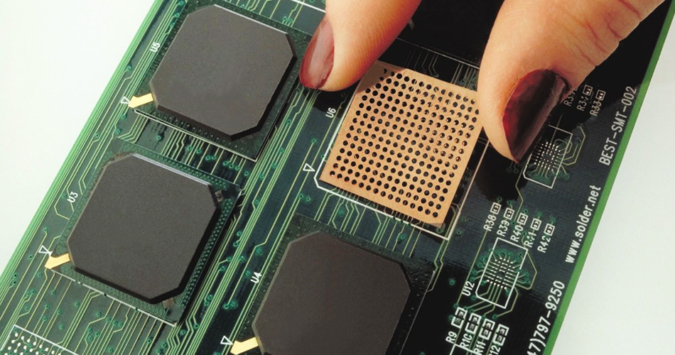
High-density packaging technology refers to the technology of installing more and smaller components on the circuit board in a limited space by using advanced packaging processes and materials. It includes packaging forms such as BGA (Ball Grid Array), CSP (Chip Scale Package), QFN (Quad Flat No-Leads), and advanced installation processes such as SMT (Surface Mount Technology).
2. Application of high-density packaging technology
High-density packaging technology is widely used in mobile phones, tablets, smart wearable devices, automotive electronics, industrial control and other fields. These products need to integrate more functions and performance in a limited space, so high-density packaging technology has become an important means to achieve product miniaturization and lightweight.
3. Advantages of high-density packaging technology
High-density packaging technology has many advantages:
High space utilization: more components can be installed in a small space to increase the functional density of the product.
Flexible circuit board layout: components can be flexibly arranged according to design requirements to increase the freedom of circuit board design.
Excellent electrical performance: packaging forms such as BGA, CSP, etc. can provide shorter signal transmission paths, reduce signal attenuation, and improve the electrical performance of the circuit.
High reliability: the use of advanced packaging processes and materials can improve the reliability and stability of components.
Easy maintenance: when a fault occurs, it is more convenient to replace a single component, reducing maintenance costs and time.
4. Challenges faced by high-density packaging technology
Although high-density packaging technology has many advantages, it also faces some challenges, such as:
Increased difficulty in soldering technology: BGA, CSP and other packaging forms have high soldering technology requirements, requiring sophisticated soldering equipment and operating skills.
Thermal management issues: High-density packaging will lead to concentrated arrangement of components, which is prone to hot spots and requires optimized heat dissipation design.
Increased design complexity: High-density packaging requires more complex circuit board design and layout, requiring designers to have a higher level of technology and experience.
5. Solutions for high-density packaging technology
In response to the challenges faced by high-density packaging technology, the following solutions can be adopted:
Optimize soldering process: Use advanced soldering equipment and technology, such as reflow soldering, lead-free soldering, etc., to ensure soldering quality and reliability.
Optimize heat dissipation design: Use heat dissipation materials such as heat sinks and heat dissipation glue to optimize the heat dissipation path and improve heat dissipation efficiency.
Strengthen design and process training: Train designers and process personnel to improve their understanding and application level of high-density packaging technology and reduce error rate and defect rate.
Summary
High-density packaging technology is of great significance in PCBA processing. It can not only improve the performance and functional density of products, but also meet consumers' demand for miniaturized and lightweight products. In the face of challenges, we can effectively solve problems by optimizing soldering processes, heat dissipation design and strengthening personnel training, so as to achieve the effective application of high-density packaging technology and promote the development and progress of the electronics manufacturing industry.
-
Delivery Service


-
Payment Options