- English
- Español
- Português
- русский
- Français
- 日本語
- Deutsch
- tiếng Việt
- Italiano
- Nederlands
- ภาษาไทย
- Polski
- 한국어
- Svenska
- magyar
- Malay
- বাংলা ভাষার
- Dansk
- Suomi
- हिन्दी
- Pilipino
- Türkçe
- Gaeilge
- العربية
- Indonesia
- Norsk
- تمل
- český
- ελληνικά
- український
- Javanese
- فارسی
- தமிழ்
- తెలుగు
- नेपाली
- Burmese
- български
- ລາວ
- Latine
- Қазақша
- Euskal
- Azərbaycan
- Slovenský jazyk
- Македонски
- Lietuvos
- Eesti Keel
- Română
- Slovenski
- मराठी
- Srpski језик
Process flow in PCBA processing
2024-10-29
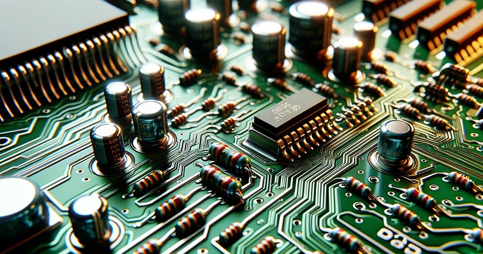
PCBA processing (Printed Circuit Board Assembly) is a crucial part of the electronic manufacturing process, involving multiple steps and technologies. Understanding the process flow of PCBA processing helps to improve production efficiency, improve product quality, and ensure the reliability of the production process. This article will introduce the main process flow of PCBA processing in detail.

1. PCB manufacturing
1.1 Circuit design
The first step in PCBA processing is circuit design. Engineers use EDA (electronic design automation) software to design circuit diagrams and generate PCB layout diagrams. This step requires precise design to ensure the smooth progress of subsequent processing.
1.2 PCB production
Manufacture PCB boards according to design drawings. This process includes inner layer graphics production, lamination, drilling, electroplating, outer layer graphics production and surface treatment. The manufactured PCB board has pads and traces for mounting electronic components.
2. Component procurement
After the PCB board is manufactured, the required electronic components need to be purchased. The purchased components must meet the design requirements and ensure reliable quality. This step includes selecting suppliers, ordering components and quality inspection.
3. SMT patch
3.1 Solder paste printing
In the SMT (surface mount technology) patch process, the solder paste is first printed on the pad of the PCB board. Solder paste is a mixture containing tin powder and flux, and the solder paste is accurately applied to the pad through a steel mesh template.
3.2 SMT machine placement
After the solder paste printing is completed, the surface mount components (SMD) are placed on the pad using a placement machine. The placement machine uses a high-speed camera and a precise robotic arm to quickly and accurately place the components in the specified position.
3.3 Reflow soldering
After the patch is completed, the PCB board is sent to the reflow oven for soldering. The reflow oven melts the solder paste by heating to form a reliable solder joint, fixing the components on the PCB board. After cooling, the solder joint re-solidifies to form a firm electrical connection.
4. Inspection and repair
4.1 Automatic optical inspection (AOI)
After the reflow soldering is completed, use AOI equipment for inspection. AOI equipment scans the PCB board through a camera and compares it with the standard image to check whether the solder joints, component positions and polarity meet the design requirements.
4.2 X-ray inspection
For components such as BGA (ball grid array) that are difficult to pass visual inspection, use X-ray inspection equipment to check the quality of internal solder joints. X-ray inspection can penetrate the PCB board, display the internal structure, and help find hidden soldering defects.
4.3 Manual inspection and repair
After automatic inspection, further inspection and repair are performed manually. For defects that cannot be identified or processed by automatic inspection equipment, experienced technicians will perform manual repairs to ensure that each circuit board meets quality standards.
5. THT plug-in and wave soldering
5.1 Plug-in component installation
For some components that require higher mechanical strength, such as connectors, inductors, etc., THT (through-hole technology) is used for installation. The operator manually inserts these components into the through holes on the PCB board.
5.2 Wave soldering
After the plug-in components are installed, a wave soldering machine is used for soldering. The wave soldering machine connects the pins of the components to the pads of the PCB board through the molten solder wave to form a reliable electrical connection.
6. Final inspection and assembly
6.1 Functional test
After all components are soldered, a functional test is performed. Use special test equipment to check the electrical performance and function of the circuit board to ensure that it meets the design requirements.
6.2 Final assembly
After the functional test is passed, multiple PCBAs are assembled into the final product. This step includes connecting cables, installing housings and labels, etc. After completion, a final inspection is performed to ensure that the appearance and function of the product meet the standards.
7. Quality control and delivery
During the production process, strict quality control is the key to ensuring the quality of PCBA. By formulating detailed quality standards and inspection procedures, ensure that each circuit board meets the requirements. Finally, qualified products are packaged and shipped to customers.
Conclusion
PCBA processing is a complex and delicate process, and every step is crucial. By understanding and optimizing each process, production efficiency and product quality can be significantly improved to meet the market demand for high-performance electronic products. In the future, as technology continues to advance, PCBA processing technology will continue to develop, bringing more innovations and opportunities to the electronics manufacturing industry.
-
Delivery Service


-
Payment Options


