
- English
- Español
- Português
- русский
- Français
- 日本語
- Deutsch
- tiếng Việt
- Italiano
- Nederlands
- ภาษาไทย
- Polski
- 한국어
- Svenska
- magyar
- Malay
- বাংলা ভাষার
- Dansk
- Suomi
- हिन्दी
- Pilipino
- Türkçe
- Gaeilge
- العربية
- Indonesia
- Norsk
- تمل
- český
- ελληνικά
- український
- Javanese
- فارسی
- தமிழ்
- తెలుగు
- नेपाली
- Burmese
- български
- ລາວ
- Latine
- Қазақша
- Euskal
- Azərbaycan
- Slovenský jazyk
- Македонски
- Lietuvos
- Eesti Keel
- Română
- Slovenski
- मराठी
- Srpski језик

EMI (electromagnetic interference) suppression methods for PCB design
Electromagnetic interference (EMI) suppression is critical to PCB design, especially in electronic devices, as it prevents electromagnetic radiation and electromagnetic susceptibility issues. Here are some common methods and techniques used to suppress electromagnetic interference:
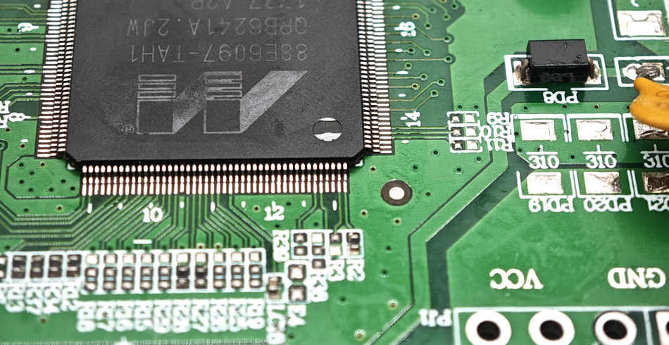
1. Ground wire planning and separation:
Use proper ground planning, including ground plane PCB design, to ensure ground loops are short and clean.
Separate grounds for digital and analog circuits to reduce mutual influence.
2. Shielding and surrounding:
Use a shielded box or shield to surround sensitive circuits to reduce the effects of external interference.
Use shields in high frequency circuits to prevent radiation.
Use shielded cables to reduce conducted interference.
3. Filter:
Use filters on power and signal lines to prevent high-frequency noise from entering or radiating from the circuit.
Add input and output filters to reduce conducted and radiated interference.
4. Layout and wiring:
Carefully plan the circuit board layout to minimize high-frequency signal paths and reduce loop area.
Minimize the length of signal lines and use differential signal transmission to reduce conducted interference.
Use a ground plane to reduce the inductance of the loop and reduce high-frequency noise.
5. Windings and inductors:
Use inductors and windings on signal lines to suppress high frequency noise.
Consider using power line filters and common mode inductors on the power lines.
6. Grounding and ground plane:
Use a low-impedance ground point and make sure all grounds on the board are connected to the same point.
Use a ground plane to provide a low impedance return path to reduce radiated and conducted interference.
7. Separation of wiring and layers:
Separate high-frequency and low-frequency signal lines and avoid them crossing on the same layer.
Use multi-layer PCB design to separate different types of signals on different levels and reduce mutual interference.
8. EMC test:
Conduct electromagnetic compatibility (EMC) testing to verify that the design complies with specified EMI standards.
Pre-test early in product development so problems can be corrected early if they arise.
9. Material selection:
Choose materials with good shielding properties, such as metals with high conductivity or special shielding materials.
Use materials with low dielectric constant and low dissipation factor to reduce conduction and radiation losses.
10. Avoid common mode problems:
Ensure differential signaling to minimize common mode noise.
Use a common mode current suppressor (CMC) to reduce common mode current.
Taking these methods and technologies into consideration can effectively suppress electromagnetic interference and ensure that PCB designs achieve the required performance and compliance in terms of EMI. Electromagnetic compatibility is a critical aspect of electronic product design and should be considered and optimized early in the design.
Send Inquiry
-
Delivery Service


-
Payment Options