
- English
- Español
- Português
- русский
- Français
- 日本語
- Deutsch
- tiếng Việt
- Italiano
- Nederlands
- ภาษาไทย
- Polski
- 한국어
- Svenska
- magyar
- Malay
- বাংলা ভাষার
- Dansk
- Suomi
- हिन्दी
- Pilipino
- Türkçe
- Gaeilge
- العربية
- Indonesia
- Norsk
- تمل
- český
- ελληνικά
- український
- Javanese
- فارسی
- தமிழ்
- తెలుగు
- नेपाली
- Burmese
- български
- ລາວ
- Latine
- Қазақша
- Euskal
- Azərbaycan
- Slovenský jazyk
- Македонски
- Lietuvos
- Eesti Keel
- Română
- Slovenski
- मराठी
- Srpski језик

Detailed explanation of PCBA processing flow: the whole process from design to manufacturing
Printed circuit board assembly (PCBA) is one of the key steps in the manufacture of electronic products. It covers multiple stages from circuit board design to component installation and final testing. In this article, we will introduce the whole process of PCBA processing in detail to better understand this complex manufacturing process.
Phase 1: Circuit board design
The first step in PCBA processing is circuit board design. At this stage, electronic engineers use PCB design software to create circuit diagrams and schematics. These drawings include various components, connections, layouts, and lines on the circuit board. Designers need to consider the size, shape, number of layers, interlayer connections, and component placement of the circuit board. In addition, they also need to follow circuit board design specifications and standards to ensure that the final PCB can meet performance, reliability, and manufacturing requirements.
Phase 2: Raw material preparation
Once the circuit board design is completed, the next step is the preparation of raw materials. This includes:
PCB substrate: usually made of glass fiber reinforced composite materials, it can be single-sided, double-sided or multi-layer boards. The material and number of layers of the substrate depend on the design requirements.
Electronic components: This includes various chips, resistors, capacitors, inductors, diodes, etc. These components are purchased from suppliers according to the BOM (Bill of Materials).
Solder: Lead-free solder is usually used to meet environmental regulations.
PCB plating material: Plating material used to coat the PCB pads.
Other auxiliary materials: such as solder paste, PCB fixtures, packaging materials, etc.
Stage 3: PCB Manufacturing
PCB manufacturing is one of the core stages of PCBA processing. This process includes:
Printing: Printing the circuit pattern on the circuit diagram onto the PCB substrate.
Etching: Using a chemical etching process to remove the unwanted copper layer, leaving the required circuit pattern.
Drilling: Drilling holes in the PCB to install through-hole components and connectors.
Electroplating: Applying conductive materials to the holes of the PCB through the electroplating process to ensure electrical connections.
Pad coating: Applying solder to the pads of the PCB for subsequent component mounting.
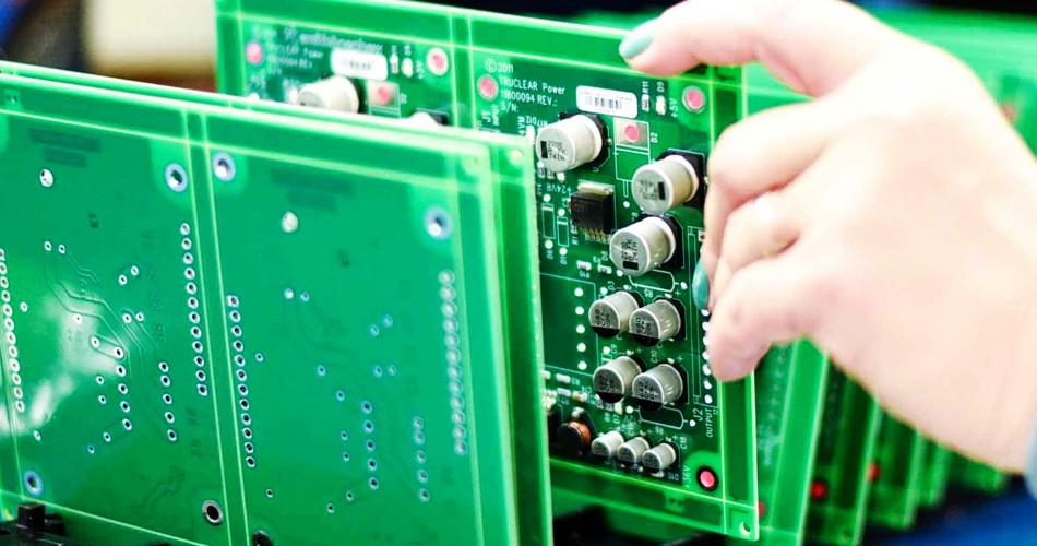
Stage 4: Component Installation
Component mounting is the process of mounting electronic components onto the PCB. There are two main component mounting technologies:
Surface mount technology (SMT): This technology involves mounting components directly on the surface of the PCB. These components are usually small and fixed to the PCB by solder paste, which is then soldered in an oven.
Thin-hole technology (THT): This technology involves inserting the pins of the component into the vias on the PCB and then soldering them in place.
Component mounting is usually performed using automated equipment such as placement machines, wave soldering machines, and hot air reflow ovens. These devices ensure that the components are accurately positioned and soldered to the PCB.
Stage 5: Testing and quality control
The next step in PCBA processing is testing and quality control. This includes:
Functional testing: Ensure that the functionality of the board meets the specifications and check the performance of the components by applying appropriate voltages and signals.
Visual inspection: Used to check the position, polarity, and soldering quality of components.
X-ray inspection: Used to check solder joints and internal connections of components, especially packages such as BGA (ball grid array).
Thermal analysis: Evaluates heat dissipation and thermal management by monitoring the temperature distribution of the PCB.
Electrical testing: Includes ICT (de-embed test) and FCT (final test) to ensure the electrical performance of the board.
Quality records: Record and track the manufacturing and testing process of each circuit board to ensure quality control.
Phase 6: Packaging and Delivery
Once the boards pass quality control and meet specifications, they are packaged. This usually involves placing the PCBs in anti-static bags and taking necessary protective measures during transportation to ensure that the boards arrive safely at their destination. The PCBs can then be delivered to the final product assembly line or customer.
Conclusion
PCBA processing is a complex and sophisticated manufacturing process that requires a high degree of technical knowledge and delicate operations. From circuit board design to component installation, to testing and quality control, each step is critical and affects the performance and reliability of the final product. Understanding the entire process of PCBA processing helps design engineers, manufacturers and customers better understand and manage all aspects of electronic product manufacturing.
Whether it is consumer electronics, medical devices or industrial automation systems, PCBA processing is the core of the modern electronics industry. By deeply understanding the process of PCBA processing, we can better respond to the evolving technology and market needs and produce high-quality, reliable and innovative electronic products.
I hope this article can help readers better understand the entire process of PCBA processing and provide valuable information for electronic engineers, manufacturers and other professionals related to PCBA.
Send Inquiry
-
Delivery Service


-
Payment Options