
- English
- Español
- Português
- русский
- Français
- 日本語
- Deutsch
- tiếng Việt
- Italiano
- Nederlands
- ภาษาไทย
- Polski
- 한국어
- Svenska
- magyar
- Malay
- বাংলা ভাষার
- Dansk
- Suomi
- हिन्दी
- Pilipino
- Türkçe
- Gaeilge
- العربية
- Indonesia
- Norsk
- تمل
- český
- ελληνικά
- український
- Javanese
- فارسی
- தமிழ்
- తెలుగు
- नेपाली
- Burmese
- български
- ລາວ
- Latine
- Қазақша
- Euskal
- Azərbaycan
- Slovenský jazyk
- Македонски
- Lietuvos
- Eesti Keel
- Română
- Slovenski
- मराठी
- Srpski језик

Gold finger technology in PCBA processing
2024-08-01
The gold finger technology in PCBA processing is a key surface treatment technology, which plays a vital role in the connection of electronic components and signal transmission. This article will introduce the gold finger technology in PCBA processing in detail, including process principles, application scenarios, advantages and precautions.
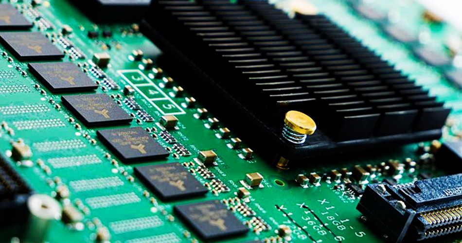
1. Process principle
The gold finger process refers to the gold plating or gold coating of specific areas on the PCB (Printed Circuit Board) circuit board to improve the reliability and stability of the connector contact. Its process principle mainly includes the following aspects:
Substrate treatment: First, the PCB substrate is surface treated, such as polishing, cleaning, etc., to ensure the adhesion and flatness of the metal layer.
Chemical treatment: The metal material is evenly deposited in the gold finger area by chemical gold plating or electroplating process to form a metal layer with good conductivity.
Protective layer treatment: After the metal layer is formed in the gold finger area, a protective layer such as nickel or alloy is usually applied to improve the corrosion resistance and service life of the gold finger.
2. Application scenarios
The gold finger process has a wide range of application scenarios in PCBA processing, mainly including but not limited to the following aspects:
Connector: used for signal transmission between connecting devices and slots, such as CPU slots, memory slots, etc.
Interface board: used to connect the interface between the PCB board and external devices or other PCB boards, such as expansion boards, interface cards, etc.
Electronic products: used for connection and communication of electronic products such as mobile phones, computers, industrial control equipment, etc.
3. Advantages
The gold finger process has the following advantages in PCBA processing:
Good conductivity: The metal layer in the gold finger area has good conductivity, which can ensure the stability and reliability of signal transmission.
Corrosion resistance: After chemical treatment and protective layer treatment, the gold finger area has strong corrosion resistance, which prolongs the service life of the connector and interface.
Connection stability: The gold finger process can improve the stability of the connector and interface, and reduce poor contact and failure during plugging and unplugging.
4. Precautions
When applying the gold finger process, the following matters need to be noted:
Process control: Strictly control each link of the gold finger process to ensure that the metal layer is uniform and the thickness is appropriate.
Protective measures: After the metal layer is formed in the gold finger area, apply a protective layer in time to prevent the metal layer from being eroded by the external environment.
Quality inspection: Perform quality inspection on the gold finger area to ensure that the conductivity and connection stability of the metal layer meet the requirements.
Conclusion
As one of the important surface treatment technologies in PCBA processing, the gold finger process can effectively improve the reliability and stability of connectors and interfaces and ensure the normal operation of electronic products. When applying the gold finger process, it is necessary to strictly control the process flow to ensure the quality and stability of the metal layer and provide reliable technical support for PCBA processing. With the continuous development of technology and the accumulation of experience, the application of gold finger technology in the field of electronic manufacturing will become more and more extensive, bringing new opportunities and challenges to the development of the industry.
-
Delivery Service


-
Payment Options