
- English
- Español
- Português
- русский
- Français
- 日本語
- Deutsch
- tiếng Việt
- Italiano
- Nederlands
- ภาษาไทย
- Polski
- 한국어
- Svenska
- magyar
- Malay
- বাংলা ভাষার
- Dansk
- Suomi
- हिन्दी
- Pilipino
- Türkçe
- Gaeilge
- العربية
- Indonesia
- Norsk
- تمل
- český
- ελληνικά
- український
- Javanese
- فارسی
- தமிழ்
- తెలుగు
- नेपाली
- Burmese
- български
- ລາວ
- Latine
- Қазақша
- Euskal
- Azərbaycan
- Slovenský jazyk
- Македонски
- Lietuvos
- Eesti Keel
- Română
- Slovenski
- मराठी
- Srpski језик

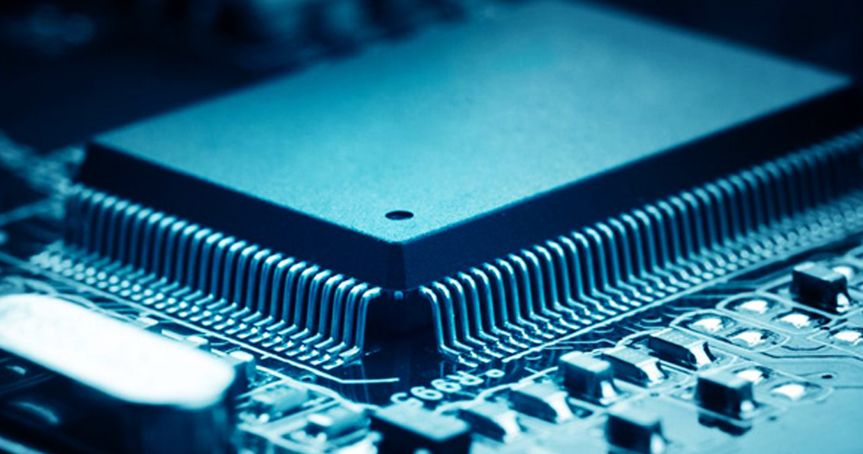
Layout Best Practices in PCBA Design: Signal Integrity and Thermal Management
2024-06-28
In PCBA design, layout is one of the key factors to ensure the signal integrity and thermal management of the circuit board. Here are some layout best practices in PCBA design to ensure the effectiveness of signal integrity and thermal management:
Best Practices for Signal Integrity:
1. Layered Layout: Use multi-layer PCBs to isolate different signal layers and reduce signal interference. Separate the power layer, ground layer, and signal layer to ensure power stability and signal integrity.
2. Short and straight signal paths: Try to shorten the signal path to reduce the delay and loss of signal transmission. Avoid long and winding signal lines.
3. Differential signal routing: For high-speed signals, use differential signal routing to reduce crosstalk and noise. Ensure that the path lengths between differential pairs are matched.
4. Ground plane: Ensure that there is enough ground plane area to reduce the return path of the signal, reduce signal noise and radiation.
5. Bypass and decoupling capacitors: Place bypass capacitors between the power pins and the ground to stabilize the power supply voltage. Add decoupling capacitors where needed to reduce noise.
6. Symmetry of high-speed differential pairs: Maintain the path length and layout symmetry of the differential pairs to ensure balanced transmission of signals.
Best practices for thermal management:
1. Thermal design: Provide sufficient heat sinks and heat dissipation paths for high-power components to effectively dissipate heat. Use thermal pads or heat sinks to improve heat dissipation.
2. Layout of heat-sensitive components: Place heat-sensitive components (such as processors, FPGAs, etc.) in suitable locations on the PCB to minimize heat accumulation.
3. Ventilation and heat dissipation space: Ensure that the chassis or housing of the PCB has sufficient vents and heat dissipation space to promote air circulation and heat dissipation.
4. Thermally conductive materials: Use thermally conductive materials such as heat sinks, thermal pads, etc. in areas where heat dissipation is required to improve heat dissipation efficiency.
5. Temperature sensors: Add temperature sensors at key locations to monitor the temperature of the PCB. This can be used to monitor and control the heat dissipation system in real time.
6. Thermal simulation: Use thermal simulation software to simulate the thermal distribution of the PCB to help optimize the layout and heat dissipation design.
7. Avoid hot spots: Avoid stacking high-power components together to prevent hot spots, which may cause overheating and failure of components.
In summary, layout in PCBA design is critical to signal integrity and thermal management. By following the above best practices, you can ensure that signals are stably transmitted on the circuit board and heat is effectively managed, thereby improving the performance and reliability of electronic products. Using circuit simulation and thermal analysis tools during the design process can help optimize the layout and solve potential problems. In addition, close cooperation with the PCBA manufacturer is also key to ensure the successful execution of the design.
-
Delivery Service


-
Payment Options