
- English
- Español
- Português
- русский
- Français
- 日本語
- Deutsch
- tiếng Việt
- Italiano
- Nederlands
- ภาษาไทย
- Polski
- 한국어
- Svenska
- magyar
- Malay
- বাংলা ভাষার
- Dansk
- Suomi
- हिन्दी
- Pilipino
- Türkçe
- Gaeilge
- العربية
- Indonesia
- Norsk
- تمل
- český
- ελληνικά
- український
- Javanese
- فارسی
- தமிழ்
- తెలుగు
- नेपाली
- Burmese
- български
- ລາວ
- Latine
- Қазақша
- Euskal
- Azərbaycan
- Slovenský jazyk
- Македонски
- Lietuvos
- Eesti Keel
- Română
- Slovenski
- मराठी
- Srpski језик

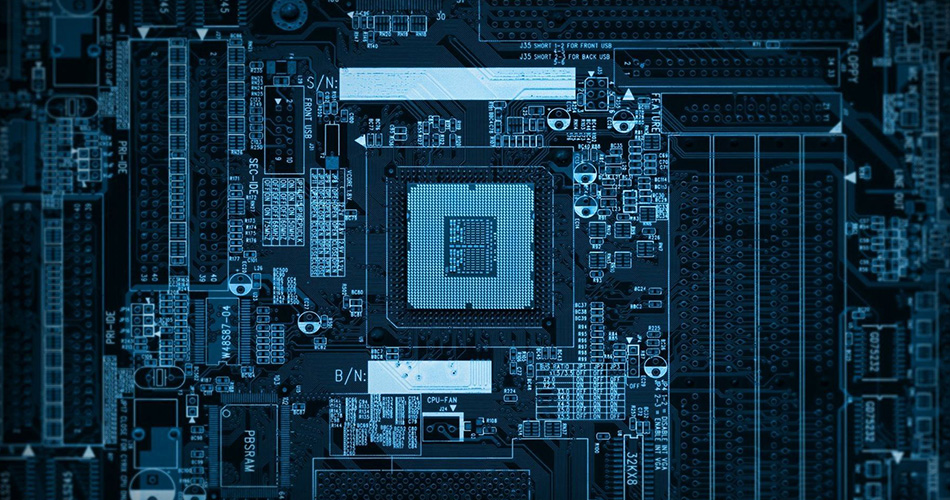
PCB design principles and layout skills: key to improving the quality of circuit board design
2024-06-30
PCB design is one of the crucial links in the modern electronic field, and good design principles and layout skills directly affect the performance, reliability, and stability of circuit boards. This article will explore some key PCB design principles and layout techniques to help engineers improve the quality of circuit board design.
1. Principles of Electromagnetic Compatibility Design
Electromagnetic compatibility is one of the important considerations in PCB design. The principles of good electromagnetic compatibility design include:
Ground wire design: Reasonably plan the return path of the ground wire to avoid the loop being too large or too long, and reduce electromagnetic interference.
Signal line planning: Try to separate and layout high-frequency signal lines from low-frequency signal lines to reduce interference between signals.
Impedance matching: For high-speed signal lines, impedance matching design is adopted to reduce signal reflection and loss.
2. Component layout and hierarchical planning
Good component layout and PCB hierarchy planning can improve the performance and stability of circuit boards:
Component layout: Place key components in appropriate positions to reduce signal transmission paths and electromagnetic interference.
PCB hierarchy planning: Reasonably plan the PCB hierarchy, separate the signal layer, power layer, and ground layer layout, and reduce signal crossing and interference.
3. PCB Design tips for power and ground wires
The design of power and ground wires is crucial for the stability and reliability of circuit boards:
Power cord width: For high-power equipment, the width of the power cord and the copper area should be considered to ensure stable current transmission.
Ground wire return path: To avoid the ground wire return path being too long or the loop being too large, and to reduce ground wire interference.
4. Wiring rules for high-speed signal lines
For the wiring of high-speed signal lines, certain rules and techniques need to be followed:
Length matching: Try to maintain high-speed signal line length matching and reduce differences in signal arrival time.
Differential signal: Using differential signal wiring to improve anti-interference ability and signal integrity.
5. Thermal management and cooling design
For high-power circuit boards, thermal management and heat dissipation design are also key design considerations:
Layout of thermal sensing components: Keep the thermal sensing components away from heat sources to avoid equipment failures caused by overheating.
Cooling design: Add cooling devices such as heat sinks, fins, or fans to ensure the normal operating temperature of the circuit board.
epilogue
The principles and layout techniques of PCB design are key factors in improving the quality of circuit board design. Engineers should have a deep understanding of electromagnetic compatibility design, component layout planning, power and ground wire design techniques, high-speed signal line routing rules, thermal management and heat dissipation design, and continuously optimize the design based on actual needs and experience to improve the performance, reliability, and stability of circuit boards.
-
Delivery Service


-
Payment Options