
- English
- Español
- Português
- русский
- Français
- 日本語
- Deutsch
- tiếng Việt
- Italiano
- Nederlands
- ภาษาไทย
- Polski
- 한국어
- Svenska
- magyar
- Malay
- বাংলা ভাষার
- Dansk
- Suomi
- हिन्दी
- Pilipino
- Türkçe
- Gaeilge
- العربية
- Indonesia
- Norsk
- تمل
- český
- ελληνικά
- український
- Javanese
- فارسی
- தமிழ்
- తెలుగు
- नेपाली
- Burmese
- български
- ລາວ
- Latine
- Қазақша
- Euskal
- Azərbaycan
- Slovenský jazyk
- Македонски
- Lietuvos
- Eesti Keel
- Română
- Slovenski
- मराठी
- Srpski језик

Do you know these 8 common PCB markings? What are their functions?
2024-07-16
1. PCB stamp hole
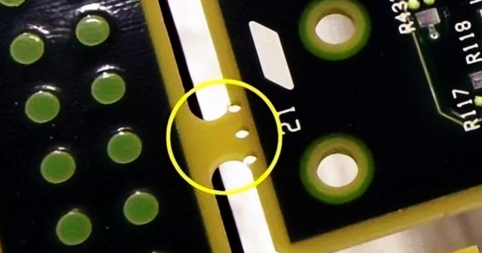
When assembling panels, in order to facilitate the separation of PCB boards, a small contact area is reserved in the middle, and the hole in this area is called a stamp hole. I personally think that the reason for the name stamp hole is that when the PCB is separated, it leaves an edge like a stamp.
2. PCB via type
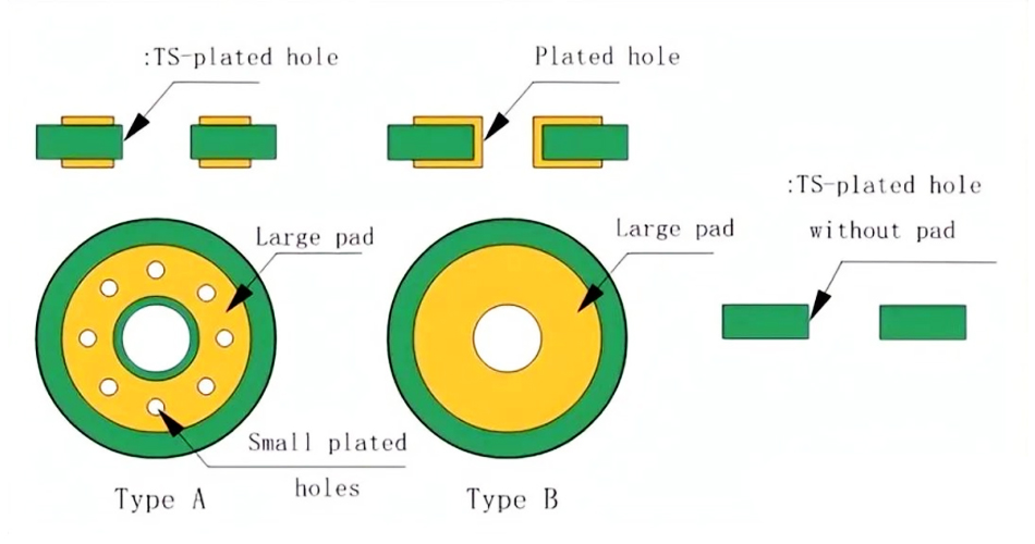
In many cases, you will see mounting holes surrounded by tiny vias. There are mainly 2 types of mounting holes here: plated and unplated. There may be 2 reasons to use surrounding vias:
1). When we want to connect the hole to the inner layer (such as GND in multi-layer PCB)
2). In the case of unplated holes, when you want to connect the upper and lower pads
3. Anti-solder pad (solder stealing)
One of the defects of wave soldering is that solder bridges are prone to occur during the soldering of SMDs. As a solution, people have found that using additional pads at the end of the original pins can solve this problem. The width of the additional pad is 2-3 times that of the ordinary pad.
Also known as solder stealing because excess solder is absorbed and solder bridges are prevented.
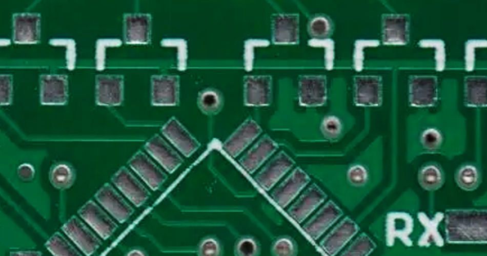
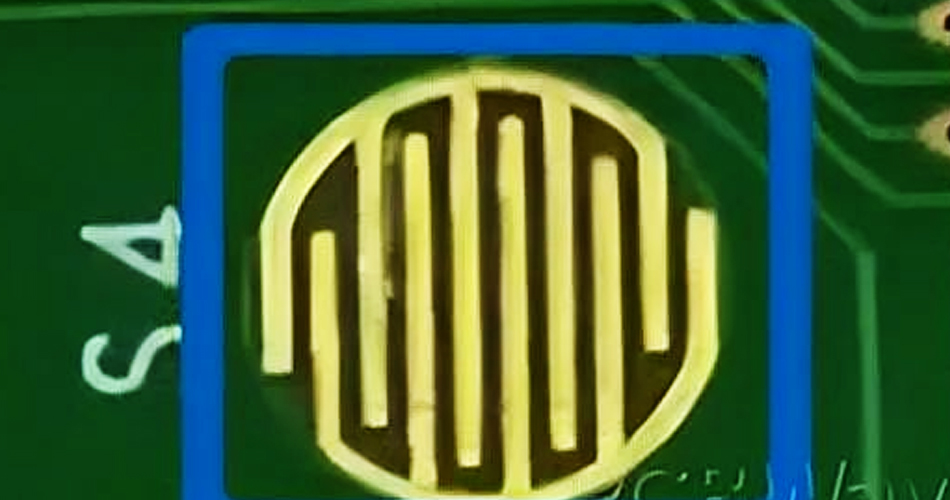
4. Fiducial Marker
A bare copper circle is inside a larger bare circle. This fiducial mark is used as a reference point for pick-and-place (PnP) machines. The fiducial mark is located in three locations:
1). In the panel.
2). Except for small pitch parts such as QFN, TQFP.
3). At the corners of the PCB.
5. Spark Gap
![]()
Spark gaps are used for ESD, current surge, and overvoltage protection. High voltage ionizes the air between the two terminals and sparks between them before damaging the rest of the circuit. This type of protection is not recommended, but it is better than nothing. The main disadvantage is that the performance will change over time.
The breakdown voltage can be calculated by the following formula: V=((3000×p×d)+1350)
Where "p" is the atmospheric pressure and "d" is the distance in millimeters.
6. PCB Conductive Keys
If you have ever disassembled a remote control or calculator, you should have seen this mark. Conductive keys consist of 2 terminals that are staggered (but not connected). When the rubber button on the keypad is pressed, the two terminals connect because the bottom of the rubber button is conductive.
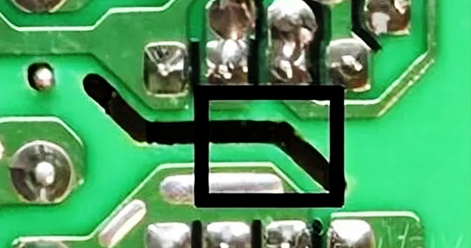
7. Fuse Tracks
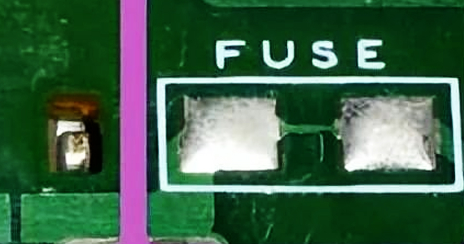
Similar to spark gaps, this is another cheap technique using PCBs. Fuse tracks are necked-down tracks on power lines and are one-time fuses. The same configuration can be used as PCB jumpers to remove specific connections by simply etching the necked-down traces (PCB jumpers can be found on the reset line on some Arduino UNO boards).
8. PCB Slotting
If you look at a high-voltage device PCB such as a power supply, you may notice air grooves between some of the traces.
Repeated temporary arcs in the PCB can cause the PCB to carbonize, resulting in a short circuit. To do this, wiring grooves can be added to the suspected area, where arcing will still occur but carbonization will not occur.
-
Delivery Service


-
Payment Options