
- English
- Español
- Português
- русский
- Français
- 日本語
- Deutsch
- tiếng Việt
- Italiano
- Nederlands
- ภาษาไทย
- Polski
- 한국어
- Svenska
- magyar
- Malay
- বাংলা ভাষার
- Dansk
- Suomi
- हिन्दी
- Pilipino
- Türkçe
- Gaeilge
- العربية
- Indonesia
- Norsk
- تمل
- český
- ελληνικά
- український
- Javanese
- فارسی
- தமிழ்
- తెలుగు
- नेपाली
- Burmese
- български
- ລາວ
- Latine
- Қазақша
- Euskal
- Azərbaycan
- Slovenský jazyk
- Македонски
- Lietuvos
- Eesti Keel
- Română
- Slovenski
- मराठी
- Srpski језик

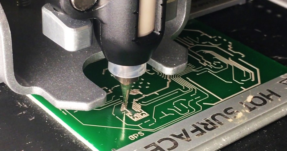
What are the design standards for PCB pads?
The design standards for PCB pads are affected by multiple factors, including application requirements, component type, manufacturing process, and number of PCB layers. Here are some common PCB pad design standards and guidelines:
1. IPC standards:
IPC (Institute for Printed Circuits) is a standards organization for the electronics manufacturing industry that publishes a series of standard documents on PCB design and manufacturing, including pad design. Common IPC standards include IPC-A-600 (Guidelines on Acceptance Criteria) and IPC-2221 (General Principles of PCB Design).
2. Component Specifications:
The design of the pads should meet the specifications and requirements of the electronic components used. Different components (such as SMD, sockets, connectors, etc.) may require different types and sizes of pads.
3. Pin spacing and arrangement:
Make sure the arrangement and spacing of the pads are adequate for the components used. Avoid overly dense layouts for reliable soldering and repairs.
4. Pad size and shape:
The size and shape of the pad should be selected based on the component's heat dissipation requirements, electrical connection requirements, and manufacturing process. Generally, SMD pads are smaller and via pads are larger.
5. Via design:
If via pads are used, make sure their location and size match the requirements of the component pins. Attention should also be paid to the filling and cover layer of the vias to prevent solder paste penetration.
6. Controlled impedance pads:
For high-frequency applications, the design of the pads may need to consider controlled impedance to ensure stable signal transmission.
7. Heat sink pads:
If a heat sink or heat dissipation component needs to be connected, the heat sink pad design should be able to effectively dissipate heat.
8. Safety spacing:
Make sure there is enough safety spacing between pads to prevent electrical shorts and other problems.
9. Pad material:
Choose appropriate pad material, usually pad plating, to ensure reliable solder connections.
10. Pad Marking:
Markings or logos can be included in the design to help assemblers and repair personnel correctly identify the function of the pad.
These standards and guidelines help ensure that the design of the circuit board pads can meet performance, reliability and manufacturing requirements. Designers often need to adjust the pad design based on specific project needs and manufacturing processes. In addition, close cooperation with manufacturers and assembly service providers can also ensure the effective implementation of pad design.
Send Inquiry
-
Delivery Service


-
Payment Options