
- English
- Español
- Português
- русский
- Français
- 日本語
- Deutsch
- tiếng Việt
- Italiano
- Nederlands
- ภาษาไทย
- Polski
- 한국어
- Svenska
- magyar
- Malay
- বাংলা ভাষার
- Dansk
- Suomi
- हिन्दी
- Pilipino
- Türkçe
- Gaeilge
- العربية
- Indonesia
- Norsk
- تمل
- český
- ελληνικά
- український
- Javanese
- فارسی
- தமிழ்
- తెలుగు
- नेपाली
- Burmese
- български
- ລາວ
- Latine
- Қазақша
- Euskal
- Azərbaycan
- Slovenský jazyk
- Македонски
- Lietuvos
- Eesti Keel
- Română
- Slovenski
- मराठी
- Srpski језик

Let's take stock of the most common mistakes in PCB design. How many of them have you made?
In the process of hardware circuit design, it is inevitable to make mistakes. Do you have any low-level mistakes?
The following lists the five most common design problems in PCB design and the corresponding countermeasures.
01. Pin error
The series linear regulated power supply is cheaper than the switching power supply, but the power conversion efficiency is low. Usually, many engineers choose to use linear regulated power supplies in view of their ease of use and good quality and low price.
But it should be noted that although it is convenient to use, it consumes a lot of power and causes a lot of heat dissipation. In contrast, the switching power supply is complex in design but more efficient.
However, it should be noted that the output pins of some regulated power supplies may be incompatible with each other, so before wiring, it is necessary to confirm the relevant pin definitions in the chip manual.
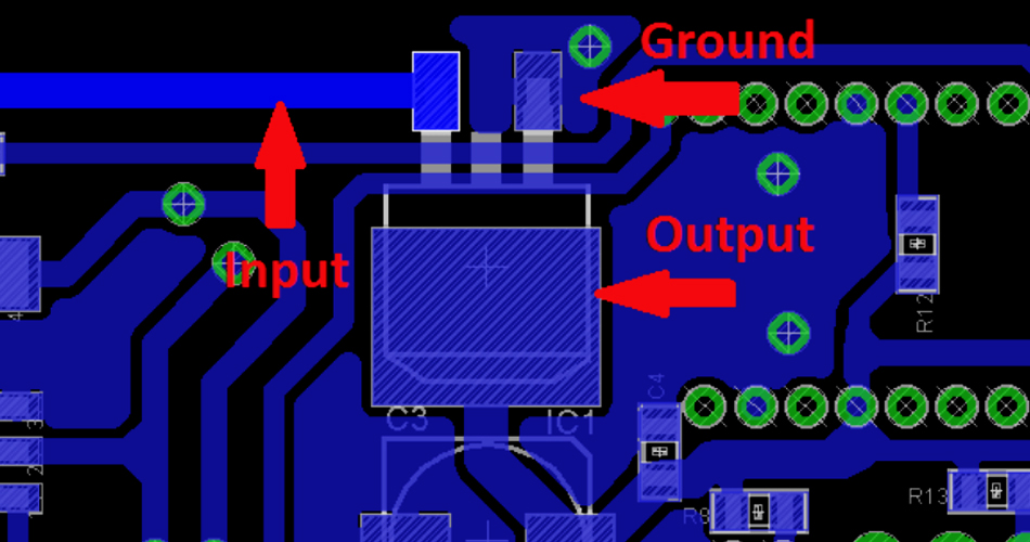
Figure 1.1 A linear regulated power supply with a special pin arrangement
02. Wiring error
The difference between design and wiring is the main error in the final stage of PCB design. So some things need to be checked repeatedly.
For example, device size, via quality, pad size and review level. In short, it is necessary to check repeatedly against the design schematic.
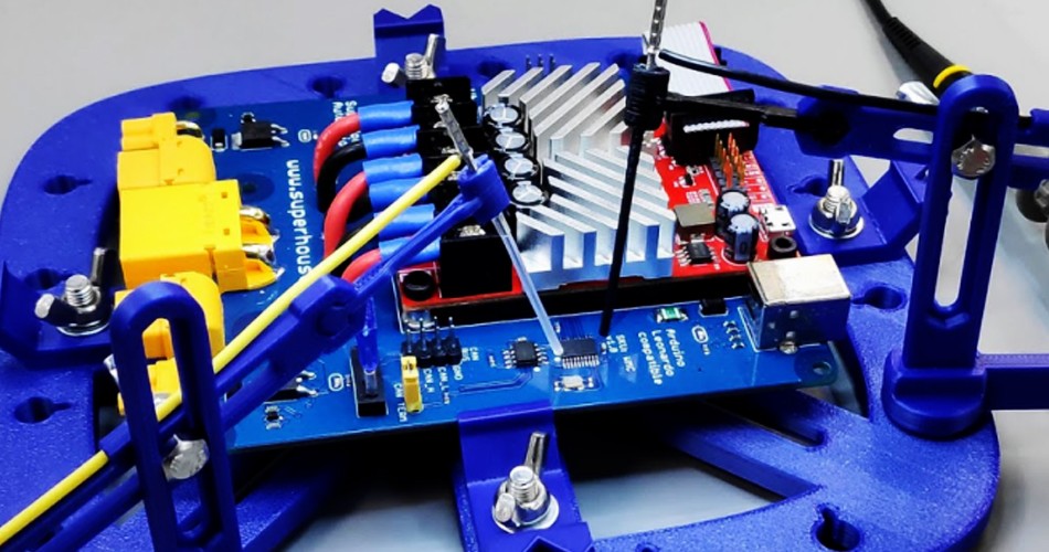
Figure 2.1 Line inspection
03. Corrosion trap
When the angle between PCB leads is too small (acute angle), an acid trap may be formed.
These acute-angle connections may have residual corrosion liquid during the circuit board corrosion stage, thereby removing more copper at that place, forming a card point or trap.
Later, the lead may break and the circuit may be open. Modern manufacturing processes have greatly reduced this corrosion trap phenomenon due to the use of photosensitive corrosion solution.
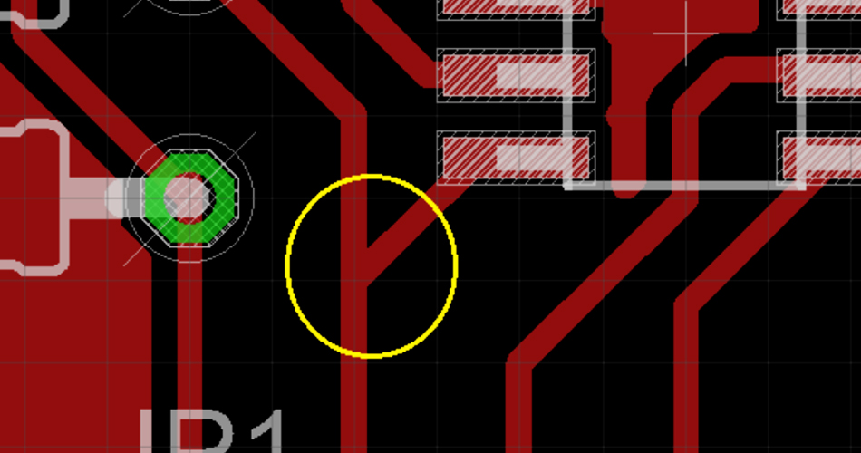
Figure 3.1 Connection lines with acute angles
04. Tombstone device
When using the reflow process to solder some small surface-mount devices, the device will form a single-end warping phenomenon under the infiltration of solder, commonly known as "tombstone".
This phenomenon is usually caused by an asymmetric wiring pattern, which makes the heat diffusion on the device pad uneven. Using the correct DFM check can effectively alleviate the occurrence of the tombstone phenomenon.
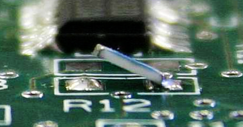
Figure 4.1 Tombstone phenomenon during reflow soldering of circuit boards
05. Lead width
When the current of the PCB lead exceeds 500mA, the PCB first line diameter will appear to be insufficient. Generally speaking, the surface of the PCB will carry more current than the internal traces of a multilayer board because the surface traces can diffuse heat through the air.
The trace width is also related to the thickness of the copper foil on the layer. Most PCB manufacturers allow you to choose different thicknesses of copper foil from 0.5 oz/sq.ft to 2.5 oz/sq.ft.

Figure 5.1 PCB lead width
Send Inquiry
-
Delivery Service


-
Payment Options