
- English
- Español
- Português
- русский
- Français
- 日本語
- Deutsch
- tiếng Việt
- Italiano
- Nederlands
- ภาษาไทย
- Polski
- 한국어
- Svenska
- magyar
- Malay
- বাংলা ভাষার
- Dansk
- Suomi
- हिन्दी
- Pilipino
- Türkçe
- Gaeilge
- العربية
- Indonesia
- Norsk
- تمل
- český
- ελληνικά
- український
- Javanese
- فارسی
- தமிழ்
- తెలుగు
- नेपाली
- Burmese
- български
- ລາວ
- Latine
- Қазақша
- Euskal
- Azərbaycan
- Slovenský jazyk
- Македонски
- Lietuvos
- Eesti Keel
- Română
- Slovenski
- मराठी
- Srpski језик

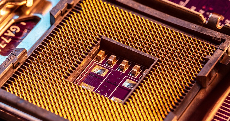
Optical microscopy inspection in PCBA processing
2024-07-23
Optical microscopy inspection in PCBA processing(Printed Circuit Board Assembly) is a critical quality control step that can effectively detect issues such as component installation, soldering quality, and surface defects on the circuit board. This article will delve into the optical microscopy inspection in PCBA processing, including its role, inspection methods, and advantages.
1. The role of optical microscopy examination
1.1 Component installation inspection
An optical microscope can enlarge the field of view and inspect the installation of components on a circuit board, including alignment and directional correctness.
1.2 Welding Quality Inspection
Inspect the welding points through an optical microscope, check the welding quality and connection condition, and avoid poor contact or short circuit problems caused by poor welding.
1.3 Surface Defect Inspection
Check the surface of the circuit board for defects such as scratches, bubbles, stains, etc., to ensure the appearance and quality of the circuit board.
2. Method of optical microscope examination
2.1 Magnification adjustment
According to the inspection requirements, adjust the magnification of the optical microscope to ensure clear observation of small components and solder joints.
2.2 Focus adjustment
Adjust the focusing device of the optical microscope to ensure clear observation focus and avoid inspection errors caused by blurring.
2.3 Field of View Movement
Move the field of view of the optical microscope to comprehensively inspect all parts of the circuit board, ensuring a thorough and comprehensive inspection.
3. The advantages of optical microscopy examination
3.1 High Resolution
Optical microscopes have high resolution and can clearly observe small components and solder joints on circuit boards, ensuring the accuracy of inspection.
3.2 Quick Inspection
Optical microscope inspection is fast and efficient, capable of conducting a comprehensive inspection of circuit boards in a short period of time, improving production efficiency.
3.3 Non destructive testing
Optical microscopy is a non-destructive testing method that does not cause damage to the circuit board and ensures its integrity.
Epilogue
Optical microscopy inspection plays a crucial role in PCBA processing, ensuring the quality and stability of circuit boards through comprehensive inspection of component installation, soldering quality, and surface defects. Optical microscopes have advantages such as high resolution, rapid inspection, and non-destructive testing, making them an indispensable quality control tool in PCBA processing.
-
Delivery Service


-
Payment Options